Tracing India's Hardware Journey: From Early Computing to Semiconductors
The Quick Read
India semiconductor history is the evolution of domestic electronics from 1950s mainframe research to modern microchip fabrication and assembly initiatives. Pioneering fabrication at Semiconductor Complex Limited in Mohali reached 5-micron nodes in 1984 before a 1989 fire halted progress, leading to today's multi-billion-dollar revitalization under the India Semiconductor Mission.
Key Takeaways
- Early computing began with indigenous mainframes like TIFRAC and ECIL's TDC-12 systems.
- Semiconductor Complex Limited produced 5-micron chips in 1984, matching early global fabrication standards.
- A catastrophic 1989 factory fire in Mohali delayed India's commercial chip production for decades.
- India commands 20% of global chip design talent despite minimal domestic front-end manufacturing.
- Current national policies target mature 28nm to 90nm nodes for automotive and industrial resilience.
Most people believe India's technology ecosystem began solely as a software export boom in the late 1990s. The truth is that India semiconductor history started decades earlier with ambitious state-funded hardware engineering and domestic silicon fabrication. Long before global tech giants set up offshore engineering centers, Indian scientists built vacuum-tube computers from scratch and fabricated microprocessors in Punjab. Understanding this technical progression explains why modern industrial policy is investing billions to reclaim lost hardware capacity. You can trace these early computing breakthroughs alongside scientific milestones in Indian history that shaped the nation's post-independence research institutions.
How Did Early Indigenous Computing Start in Post-Independence India?
India entered computing in the 1950s by building indigenous mainframes at research institutions to support atomic energy and national planning. Spearheaded by Homi Bhabha at the Tata Institute of Fundamental Research, projects like TIFRAC and ECIL's TDC-12 proved domestic teams could build complex hardware without relying entirely on foreign turnkey systems.
+-------------------------------------------------------------------------+
|                  EARLY INDIAN COMPUTING MILESTONES                      |
+-------------------------------------------------------------------------+
|  1954: Homi Bhabha initiates computer development team at TIFR         |
|  1956: Pilot unit operational; full TIFRAC mainframe running by 1960    |
|  1967: Electronics Corporation of India Limited (ECIL) founded          |
|  1969: ECIL builds TDC-12, India's first commercial transistorized CPU  |
+-------------------------------------------------------------------------+
The TIFRAC Breakthrough at Colaba (1956–1960)
The TIFRAC breakthrough is the development of India's first indigenous full-scale digital mainframe computer between 1956 and 1960 at the Tata Institute of Fundamental Research in Colaba, Mumbai. Spearheaded by Homi Bhabha and lead engineer Professor R. Narasimhan, the project established domestic capabilities in logic circuitry, memory cores, and digital computing for atomic research.
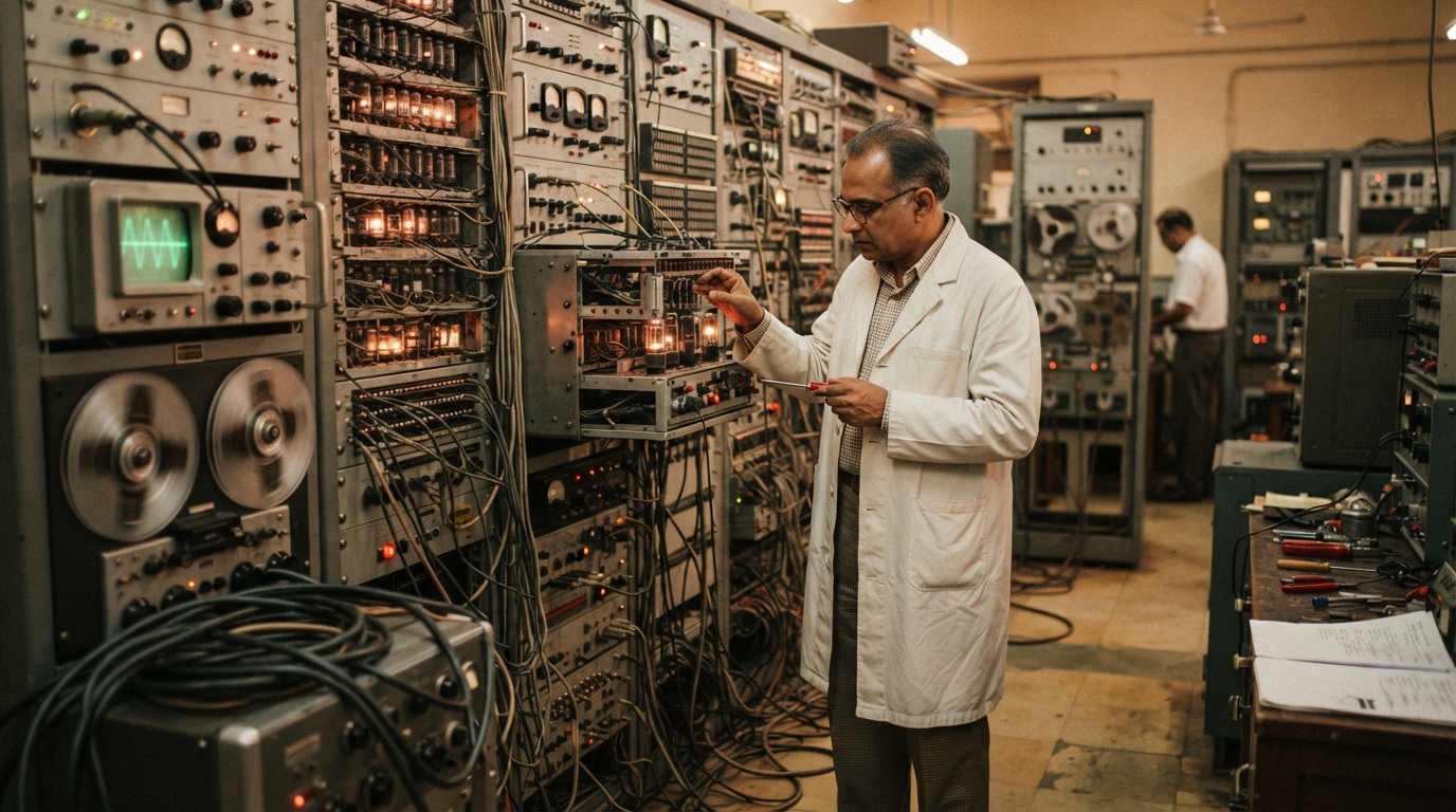
The modern computational story began inside the Old Yacht Club building in Colaba, Mumbai. In 1954, Homi Bhabha recognized that calculating nuclear reactions required automated computing machines that India could not readily import. Homi Bhabha gathered a small team of physicists and engineers under Professor R. Narasimhan to design a full-scale digital computer.
The team commissioned a pilot test unit in 1956 before completing the main system in 1960. The team named the machine the Tata Institute of Fundamental Research Automatic Calculator, or TIFRAC. The system used over 1,000 vacuum tubes, crystal diodes, and an auxiliary magnetic drum memory. TIFRAC operated at a clock speed that solved complex differential equations in minutes rather than weeks.
TIFRAC was not just a theoretical experiment. Indian scientists used the mainframe daily to calculate atomic shield thicknesses, weather simulations, and demographic models. Prime Minister Jawaharlal Nehru formally named the machine in January 1962, marking India's arrival in electronic computing. The project showed Indian engineers how to design logic circuits, memory cores, and input-output systems from basic components.
ECIL and the Commercialization of the TDC-12
The TDC-12 is India's first commercial transistorized digital computer, developed in 1969 by the Electronics Corporation of India Limited (ECIL) in Hyderabad under Vikram Sarabhai's leadership. Built for industrial process control, power stations, and defense networks, the 12-bit system demonstrated that domestic public enterprises could successfully mass-produce solid-state electronics for mission-critical national operations.
Building custom research mainframes was an important first step. The Indian government needed standardized commercial computers for industrial process control, power stations, and defense networks. In 1967, the Department of Atomic Energy established the Electronics Corporation of India Limited (ECIL) in Hyderabad under Vikram Sarabhai's guidance.
ECIL took laboratory designs and turned them into factory-produced commercial machines. By 1969, the public enterprise unveiled the TDC-12, India's first commercial transistorized computer. The 12-bit system executed up to 250,000 additions per second. The TDC-12 ran without vacuum tubes, using solid-state germanium and silicon transistors mounted on printed circuit boards.
ECIL delivered TDC-12 systems to defense laboratories, university physics departments, and the Indian Space Research Organisation (ISRO). The hardware was durable and handled India's erratic power supply and high ambient temperatures. ECIL followed with the TDC-16 and TDC-316 in the 1970s. These machines ran real-time tracking systems for radar installations and railway logistics. This period proved that domestic factories could produce operational electronics for mission-critical national operations.
Academic Computing and the Arrival of Mainframes
While ECIL focused on industrial computers, academic institutions required machines for teaching and theoretical research. The Indian Institute of Technology (IIT) Kanpur took the lead in 1963 by installing an IBM 1620 mainframe. The system arrived via a transport aircraft as part of the Kanpur Indo-American Program.
The installation established the first formal computer science curriculum in India. Students typed instructions on punched cards and waited overnight for compilation runs. Similar installations followed at IIT Madras with an IBM 1130 and IIT Bombay with a Soviet Minsk-2 mainframe.
These university labs trained the initial cadre of Indian system designers and hardware engineers. Students learned machine-level assembly programming, electrical bus architectures, and circuit design. The academic push created a generation of technical specialists who later staffed domestic public sector manufacturing units and foreign research centers.
What Happened to India's First Silicon Fab at SCL Mohali?
India established Semiconductor Complex Limited (SCL) in Mohali in 1976 to build indigenous microprocessors and telecommunications chips. By 1984, SCL fabricated 5-micron silicon wafers, putting India only two generations behind global leaders before a devastating 1989 factory fire abruptly ended commercial operations.
+-------------------------------------------------------------------------+
|                  THE RISE AND FALL OF SCL MOHALI                        |
+-------------------------------------------------------------------------+
|  1976: Semiconductor Complex Limited (SCL) established in Punjab        |
|  1984: Commercial fabrication begins at 5-micron (5,000 nm) node        |
|  1987: SCL advances process node to 3-micron technology                 |
|  1989: Catastrophic cleanroom fire destroys primary production line     |
|  1997: Reconstruction finishes; commercial market window closed         |
+-------------------------------------------------------------------------+
Operating on the Global Frontier in 1984
The founding of Semiconductor Complex Limited in SAS Nagar (Mohali), Punjab, represented an ambitious effort to enter front-end microelectronics. The facility began commercial production in 1984, three years before Taiwan Semiconductor Manufacturing Company (TSMC) was founded in Taiwan.
The Indian government negotiated technology transfer agreements with American Microsystems and Rockwell International. SCL engineers quickly mastered the fabrication process. In 1984, SCL manufactured chips using a 5-micron (5,000 nm) fabrication node [Carnegie Endowment, 2025]. For comparison, global market leaders like Intel were fabricating processors at 3-micron and 1.5-micron nodes during the same period. SCL narrowed the gap to a 3-micron process by 1987.
The Mohali facility produced digital watch modules, electronic telephone exchange circuits, and custom logic chips. The plant also fabricated the 6502 microprocessor under license, which powered popular home microcomputers like the BBC Micro and Apple II. Domestic fabrication allowed Indian telecommunication networks to replace electro-mechanical switches with digital integrated circuits made in Punjab.
The 1989 Fire and Eight Years of Stagnation
On February 7, 1989, a catastrophic fire swept through the SCL facility in Mohali [YourStory, 2026]. The fire gutted the complex, incinerating the cleanrooms, silicon wafer processing equipment, testing bays, and precision lithography machines.
The physical destruction was total, but the administrative delay was worse. Bureaucratic hurdles and budget delays postponed reconstruction for years. It took eight full years for the government to rebuild and reopen the SCL facility in 1997 [YourStory, 2026].
In semiconductor manufacturing, an eight-year gap is an eternity. By 1997, the global industry had migrated to sub-micron fabrication nodes, 200mm silicon wafers, and automated manufacturing tools. SCL could not catch up with private global foundries that were spending billions every year on research and development. The rebuilt plant lost its commercial edge and turned into a captive foundry, manufacturing specialized radiation-hardened chips for ISRO launch vehicles and defense systems.
The Strategic Lessons of the Mohali Setback
The Mohali setback is the long-term loss of domestic microchip manufacturing momentum following a catastrophic February 1989 cleanroom fire at Semiconductor Complex Limited in Punjab. The event demonstrated that semiconductor fabrication requires continuous multi-billion-dollar capital reinvestment, uninterrupted utilities, and rapid administrative decision-making to survive fast global node migration and avoid total market obsolescence.
The loss of SCL Mohali altered India semiconductor history permanently. The loss showed that silicon foundries cannot survive through intermittent state grants. Microchip fabrication requires constant capital expenditures, uninterrupted cleanroom power, and supply chain redundancy.
When SCL went down, domestic electronics brands had to import integrated circuits from Japan, South Korea, and Taiwan. The disaster broke the continuous cycle of process learning that chip technicians need. The disruption also discouraged private Indian capital from entering chip manufacturing for three decades. Foundries were seen as capital pits with high technology risk. This single factory fire shifted the country's technology trajectory from manufacturing silicon to writing the software that runs on it.
Why Did India Shift from Hardware Manufacturing to Software Exports?
Economic liberalization in 1991 altered India's technological trajectory by prioritizing low-capital software engineering over expensive hardware foundries. High customs duties, infrastructure deficits, and lengthy capital recovery cycles pushed entrepreneurs into services, creating a massive chip design talent base without domestic fabrication lines.
+-------------------------------------------------------------------------+
|                  THE SHIFT FROM SILICON TO SOFTWARE                     |
+-------------------------------------------------------------------------+
|  Hardware Fab Challenges (1990s)    |  Software Services Boom (1990s)   |
+-------------------------------------+-----------------------------------+
|  $1B+ initial factory setup costs   |  Low startup capital requirements |
|  Heavy cleanroom water/power needs  |  Export revenues via satellite    |
|  High customs tariffs on components |  Tax exemptions on IT exports     |
|  Rapid 3-year node obsolescence     |  High gross operating margins     |
+-------------------------------------+-----------------------------------+
The Post-1991 Economic Pivot
The balance-of-payments crisis in 1991 forced sweeping structural reforms across the national economy. The government devalued the rupee and removed import quotas. You can read more about how these changes unfolded across the country in our guide on economic milestones in Indian history.
For the technology sector, economic liberalization created immediate incentives for software development. Building a semiconductor fab required over $1 billion in upfront capital, uninterrupted electricity, millions of gallons of ultrapure water, and imported chemical inputs. By contrast, launching a software consultancy required only office space, desktop workstations, and a satellite communications link.
Software firms earned foreign currency with high operating margins and zero factory risk. State policies adapted by creating Software Technology Parks of India (STPI) with tax holidays and duty-free hardware imports. Capital followed this path of least resistance. Private enterprise turned toward software services, back-office operations, and enterprise software integration, leaving domestic hardware fabrication unfunded.
The 20% Design Talent Paradox
While India stepped back from chip fabrication, global technology firms realized Indian engineers were exceptional at chip design. Designing an integrated circuit requires mathematical modeling, logic design, and verification. These tasks happen on specialized software workstations rather than in cleanrooms.
Texas Instruments opened its pioneering Bangalore design center in 1985. Intel, Cadence, Synopsys, Qualcomm, and Nvidia followed over the next two decades. Today, India accounts for roughly 20% of the world’s semiconductor design workforce [Bisinfotech, 2026]. Engineers in Bengaluru, Hyderabad, and Noida help design high-performance processors used in consumer smartphones, graphics units, and server hardware.
This situation created a structural paradox. Indian engineers design many of the world's most complex microchips, yet domestic factories could not manufacture a single commercial wafer. Every design file had to be sent abroad to foundries in Taiwan, South Korea, or the United States for tape-out and physical manufacturing.
| Dimension | Semiconductor Design (Fabless) | Front-End Fabrication (Foundry) |
|---|---|---|
| Capital Requirement | Low to moderate ($5M–$50M for tooling) | Very high ($5B–$15B per fab line) |
| Physical Infrastructure | Standard engineering office, high-compute servers | Vibration-isolated cleanroom, ultrapure water |
| India's Global Share | ~20% of global talent [Bisinfotech, 2026] | <1% of global wafer capacity [Bisinfotech, 2026] |
| Primary Risk | Intellectual property and software bugs | Node obsolescence, wafer defects, machine downtime |
| Key Indian Hubs | Bengaluru, Hyderabad, Noida, Pune | Dholera, Sanand, Mohali |
Infrastructure Deficits in Early Manufacturing
The infrastructure deficit in early Indian manufacturing is the lack of reliable electric power, ultrapure water supplies, and favorable tariff structures that prevented private semiconductor fabrication during the 1990s and 2000s. Because wafer production requires uninterrupted power grids and millions of daily gallons of water, infrastructural instability forced India to become an electronics consumer rather than a producer.
The failure to build private fabs in the 1990s and 2000s came down to infrastructure and trade policy. A commercial fab consumes between 2 to 5 million gallons of ultrapure water daily and requires steady electric power. Voltage fluctuations of a few milliseconds can ruin an entire production batch of silicon wafers.
Indian industrial parks in the late 1990s could not guarantee this grid reliability. Inverted duty structures also made importing finished electronic goods cheaper than manufacturing components domestically. Component assembly suffered alongside fabrication. India became a consumption market for foreign hardware while remaining an export center for digital services.
How Is the India Semiconductor Mission Rebuilding Domestic Capacity?
The India Semiconductor Mission (ISM) provides financial subsidies covering up to 50% of project capital costs to establish local fabs and packaging units. Backed by ₹1.64 lakh crore in sanctioned investments, the program focuses on mature node manufacturing and outsourced assembly to secure critical supply chains.
+-------------------------------------------------------------------------+
|                  INDIA SEMICONDUCTOR MISSION (ISM)                      |
+-------------------------------------------------------------------------+
|  Fiscal Incentive: 50% central support on capital expenditure           |
|  Total Approved Projects: 12 facilities across fabs and OSAT units      |
|  Sanctioned Capital: ₹1.64 lakh crore (~$19.7B) [UJA, 2026]             |
|  ISM 2.0 Allocation: ₹1,27,500 crore for supply chain inputs [UJA, 2026] |
+-------------------------------------------------------------------------+
Mature Nodes: The Strategic 28nm to 90nm Choice
A common misconception in chip manufacturing is that a country must build sub-3nm chips to be competitive. Leading-edge nodes power flagship smartphones and artificial intelligence accelerators, but mature nodes make up the bulk of global industrial volume.
The Indian government directed initial foundry subsidies toward mature nodes between 28nm and 90nm. Modern electric vehicles, industrial robotics, power grids, and defense hardware rely heavily on mature microcontrollers and power management chips. These nodes require lower capital expenditures, achieve higher production yields faster, and remain commercially viable for decades.
The cornerstone project of this strategy is the Tata Electronics and Powerchip Semiconductor Manufacturing Corporation (PSMC) joint venture in Dholera, Gujarat [Carnegie Endowment, 2025]. The $10 billion commercial fab is designed for 300mm silicon wafers with a capacity of up to 50,000 wafer starts per month. The plant targets 28nm, 40nm, and 90nm logic and power management integrated circuits [ET CIO, 2026]. This focus directly supplies automotive and power electronics manufacturers without competing against high-risk leading-edge foundries.
Packaging and Assembly: The OSAT and ATMP Foundation
Building a full front-end silicon fabrication plant takes years of construction and process calibration. To establish industrial momentum quickly, the India Semiconductor Mission prioritized back-end packaging through Outsourced Semiconductor Assembly and Test (OSAT) and Assembly, Testing, Marking, and Packaging (ATMP) units.
In back-end packaging, processed silicon wafers are cut into individual dies, wired onto substrate frames, and encapsulated in protective resin. These units require less capital than front-end fabs while generating local supply chain jobs. Micron Technology established a prominent packaging facility in Sanand, Gujarat, to assemble dynamic RAM and flash memory modules [ET CIO, 2026].
Additional packaging facilities from domestic firms like CG Semi and Kaynes Semicon have expanded assembly capacity across multiple states [ET CIO, 2026]. Union Minister for Electronics and IT Ashwini Vaishnaw noted that this approach creates a full-stack ecosystem, establishing packaging lines while foundries complete construction [Press Information Bureau (PIB), 2026].
Policy Outlays and ISM 2.0
The initial phase of the India Semiconductor Mission allocated ₹76,000 crore ($10 billion) in fiscal support, offering up to 50% co-funding on capital costs. State governments matched these packages with additional utility subsidies, discounted land, and water infrastructure. By 2026, cumulative sanctioned investments across 12 approved projects reached ₹1.64 lakh crore (~$19.7 billion) [UJA, 2026] [dholeraSTOP, 2026].
Building on this progress, the government introduced ISM 2.0 with an expanded policy outlay of ₹1,27,500 crore [UJA, 2026]. ISM 2.0 shifts policy focus upstream. It provides financial incentives for:
- Semiconductor manufacturing equipment and spare parts
- Specialty chemical producers and ultra-pure industrial gases
- Design-Linked Incentive (DLI) programs supporting indigenous intellectual property
- Advanced research centers focused on wide-bandgap semiconductors like Gallium Nitride (GaN) and Silicon Carbide (SiC)
These upstream subsidies protect factories from sudden supply disruptions. India's domestic semiconductor market is projected to reach $100–110 billion by 2030 [Press Information Bureau (PIB), 2026]. Building domestic supply chains helps capture this value rather than spending foreign reserves on component imports.
What Are the Key Milestones in India Semiconductor History?
The timeline of Indian semiconductor development spans over seven decades of technical experimentation, institutional setbacks, and industrial policy overhauls. From early university mainframes to multi-billion-dollar wafer fabs, these pivotal dates reflect India's ongoing pursuit of hardware self-reliance across critical technological eras.
+-------------------------------------------------------------------------+
|                  SEVEN DECADES OF HARDWARE MILESTONES                   |
+-------------------------------------------------------------------------+
|  1956: TIFRAC computational pilot system operational in Mumbai          |
|  1969: ECIL builds TDC-12 solid-state minicomputer                      |
|  1976: Semiconductor Complex Limited (SCL) incorporated                 |
|  1984: SCL Mohali runs 5-micron commercial chip line                    |
|  1989: Mohali cleanroom fire disrupts domestic fab capacity            |
|  1991: Economic reforms accelerate software exports over hardware       |
|  2021: India Semiconductor Mission (ISM) launched with ₹76,000 crore    |
|  2024: Construction begins on Tata-PSMC commercial fab at Dholera       |
|  2026: ISM 2.0 expands incentives upstream to chemicals and tooling     |
+-------------------------------------------------------------------------+
Chronological Timeline: 1956 to 2026
To understand how domestic hardware manufacturing evolved, you can examine these key historical dates in India semiconductor history alongside historic dates in modern India.
| Year | Milestone Event | Technology Focus | Strategic Significance |
|---|---|---|---|
| 1956 | TIFRAC development begins at TIFR Mumbai | Vacuum tubes, ferrite memory | Established indigenous electronic design capabilities. |
| 1969 | ECIL produces the TDC-12 | Transistor logic, 12-bit architecture | First commercial solid-state computer produced in India. |
| 1976 | Incorporation of SCL Mohali | Silicon wafer processing | First state-directed microelectronics initiative. |
| 1984 | SCL achieves 5-micron production | 5,000 nm CMOS / NMOS chips | Narrowed the gap with global semiconductor foundries. |
| 1989 | SCL cleanroom fire | Cleanroom infrastructure | Commercial fabrication stopped for nearly a decade. |
| 1991 | Liberalization and STPI formation | Software services, design tools | Capital shifted from factory hardware to IT exports. |
| 2006 | SCL restructured under Department of Space | Radiation-hardened microchips | Dedicated facility to supply space and defense hardware. |
| 2021 | Launch of India Semiconductor Mission | Capital subsidies (50% fiscal support) | Modern industrial policy supporting private fabrication. |
| 2024 | Groundbreaking at Dholera Fab | 28nm, 40nm, 90nm nodes | First private commercial 300mm wafer fab in India. |
| 2026 | Implementation of ISM 2.0 | Tooling, gases, and indigenous IP | Expanded subsidies to upstream supply chain inputs. |
Analyzing Past Failures Versus Modern Execution
Past Indian semiconductor initiatives often faltered during execution. As Konark Bhandari of Carnegie India observed, previous efforts suffered from uneven and false starts [Carnegie Endowment, 2025]. Earlier policies offered modest tax breaks or non-binding letters of intent. When global market cycles turned down, international chipmakers routinely canceled their planned Indian investments.
The current strategy differs in three distinct ways:
- Direct Capital Support: The government pays cash subsidies up to 50% of capital expenditure as milestones are built, rather than offering delayed tax deductions.
- Infrastructure Readiness: Industrial parks like Dholera and Sanand feature dedicated water canals, uninterruptible power substations, and multi-modal logistics links built before foundry construction.
- Anchor Domestic Demand: Local electronics manufacturing production has grown substantially, creating an immediate domestic market for power ICs, microcontrollers, and memory packages.
You can learn more about how domestic research programs adapted during this era in our detailed overview of the history of India's space program hardware.
Frequently Asked Questions
Q: Why did India fall behind in semiconductor manufacturing during the 1990s? The 1989 fire at SCL Mohali halted domestic fabrication for eight years. During the same period, 1991 economic reforms created high returns in software exports with minimal capital requirements. High import tariffs, unstable power grids, and cleanroom water shortages also discouraged private investors from building local wafer foundries.
Q: What is the difference between mature nodes and advanced nodes in India's chip strategy? Advanced nodes (sub-5nm) are used primarily in flagship smartphone processors and high-end AI accelerators, requiring hundreds of billions in capital. Mature nodes (28nm to 90nm) power cars, industrial machines, home appliances, and power grids. India targets mature nodes because they require lower initial capital and match current domestic manufacturing demand.
Q: How large is India's domestic semiconductor market expected to grow? The domestic semiconductor market is projected to reach between $100 billion and $110 billion by 2030 [Press Information Bureau (PIB), 2026]. This growth is driven by consumer electronics assembly, automotive electrification, industrial automation, and expanding wireless telecommunications infrastructure.
Q: What role did Semiconductor Complex Limited (SCL) play in India's space program? After its commercial operations ceased following the 1989 fire, SCL was reorganized under the Department of Space in 2006. The Mohali fab pivoted to manufacturing custom radiation-hardened microchips, sensor units, and image processors for ISRO launch vehicles, satellites, and national defense programs.
Your next move is to track commercial yield timelines rather than policy announcements. If you are sourcing electronics or investing in supply chains, verify when the Dholera fab completes test wafer runs for 28nm circuits in 2026. Prioritize partnerships with domestic packaging and OSAT units in Sanand today, as these facilities will reach full commercial volume well before front-end foundries stabilize.
Related Reading
- India at the Olympics: A Timeline of Historic Sporting Milestones
- Milestones in Indian Women's History: A Chronological Guide
- 1,000 Years of Indian Medical History: A Chronological Guide
- Economic Milestones in Indian History: From 1947 to Present
Sources
- TIFRAC, India's First Computer - A Retrospective — Indian Academy of Sciences, 2008. Supports: The development and commissioning of India's first digital mainframe computer, TIFRAC, at the Tata Institute of Fundamental Research between 1956 and 1960.
- India's chip dream was derailed in 1989. In 2026, it's roaring back — YourStory, 2026. Supports: SCL Mohali initiating 5-micron chip fabrication in 1984, the catastrophic February 7, 1989 cleanroom fire, and the eight-year delay before restarting operations in 1997.
- India has emerged as a global hub for semiconductor design and R&D — Press Information Bureau, 2026. Supports: India employing approximately 20% of the world's semiconductor chip design workforce and hosting 7% of global semiconductor Capability Centres.
- Tata Group to Build the Nation's First Fab in Dholera — Tata Group, 2024. Supports: Tata Electronics partnering with PSMC to construct a commercial semiconductor fabrication plant in Dholera with a capacity of up to 50,000 wafer starts per month.
- India Building Semiconductor Future: Emerging Capabilities Across Design, Manufacturing, Packaging, Materials and Talent — Press Information Bureau, 2026. Supports: The Union Cabinet approval of Semicon 2.0 with a ₹1,27,500 crore outlay focusing on chip design, equipment, raw materials, and advanced packaging.
- India Semiconductor Mission 2.0 — Press Information Bureau, 2026. Supports: Industry projections estimating the Indian domestic semiconductor market will grow to between $100 billion and $110 billion by 2030.